The PCB design is both an art and a science. And the component placement is the artistic side which makes it more interesting and satisfying. If you give the design to ten engineers you will get 10 different layouts for the same PCB with some unique characteristics. It is unlike the schematic where it all boils down to underneath mathematics and physics. In reality, there is no “Right way” for component placement. It doesn’t mean one can do anything they want. But still, it is a great puzzle which requires creative effort.

There is a common saying that the component placement is 90% of the PCB layout. Proper Placement of components in PCB simplifies the design to a much extent. This also helps in the preservation of signal by lowering noise in much possible way. In general, we are provided with the reference design as application notes from the component vendor. It is always better to follow guidelines from the manufacturer. In some cases, we need to make some changes or if a reference design is not available we can apply some common principles and tips to get through this phase.
1. Understand the constraints
1.1. Mechanical Constraints
Even before placing any component it is needed to understand the mechanical constraints. This will help to decide which are the places where one is not supposed to place the component or at some certain place/side there is a limitation of height. It is must to get few questions answered before starting. e.g.
- What is the outline of the board?
- What are the places for mounting holes?
- What are the other mechanical fixtures (e.g. heat-sink, other support assemblies) which are going to occupy the real estate in the board?
- What are the required clearances?
- What are the restrictions on components placement (e.g. Where are the connectors/heat-sink are required to be placed as per over-all design)?
Place the edge component first. If the mechanical design is already prepared then the position of these components are stoned. This is an easy point to start with in all the process. Although if possible please suggest few guidelines for edge component placement based on EMI/EMC certification requirements. Some of the constraints are mentioned in the circuit constraint section, but the details can be extracted from our article 15 PCB Layout guidelines to achieve EMC requirements.
1.2. Manufacturing and testing related constraints
Once the basic questions are answered designer has to think in terms of manufacture-ability. And this gives rise to new set of questions.
- What are the restrictions from the manufacturing partner(e.g. How close pads should be so that there are no chance of short? e.t.c)
- What are the restrictions from the assembly house?
- How the board is going to be assembled and tested(manual or machine)?
- Which soldering method is going to be used?
These questions will shape multiple design decisions. e.g. if components are placed on conveyor belt they are far from the edge so that no damage occurs during assembly. If they are being tested automatically all test points should be on one side of the PCB depending on test equipment. Same-way if manual testing is planned all test points should be on top and easily accessible to test engineer.
1.3. Understand the circuit constraints
Before going to start further its better to understand some circuit constraints which are necessary to for higher signal to noise ratio(SNR). understanding these constraints will help in grouping of components, and significantly increase the reliability of design.
- Current requirement: Higher current consuming parts are better placed near power supply as we don’t want the board to heat-up un-necessarily. Heat up will give rise to thermal noise. Also, it is better to place these parts away from the sensitive circuit. Switching supply should be also filtered properly and better placed in an isolated corner/side.
- Clock: The thumb rule is: “Be paranoid about clock”. Same goes for high-speed digital signals, as these can also be characterized as clocks. Component placement should be planned to minimise these trace lengths. It is better to keep in mind that series termination should be placed near source while parallel termination near the sink.
- Multiple frequencies: Never Mix Low frequency and High-frequency components together. Place them separately.
- Noise Immunity: Keep at least 200mil clearance from the transformer/choke to the electrolytic capacitor.
- Decoupling: Placement of decoupling capacitors near the “power pin” of ICs have to be assured. This will help in achieving better power integrity, i.e. lesser fluctuation in power line.
- Ground Bounce: Ground bounce between two off-board connectors can create enough radiation for it to fail the EMI/EMC testing. This can be reduced if no high-speed digital component is placed between two connectors. If there is no mechanical constraint, it is better to place connectors together on one side of the board.
2. Group the components
2.1. Create a modular design
Good component placement is supposed to reduce the routing complexity. So it is advisable to group the components in small logical groups same as a schematic. Start placing by larger IC’s. And then place support component like resistors, capacitors around them. Each such device will have a separate classifiable group. Grouping can be visualised as the modules in the whole design. It is beneficial for one to one comparison with the schematic. This will also help in future work as the same set can be used in other design as a template. While grouping the components one should put attention to minimize the intersection of signals.
2.2. Group analog and digital parts carefully
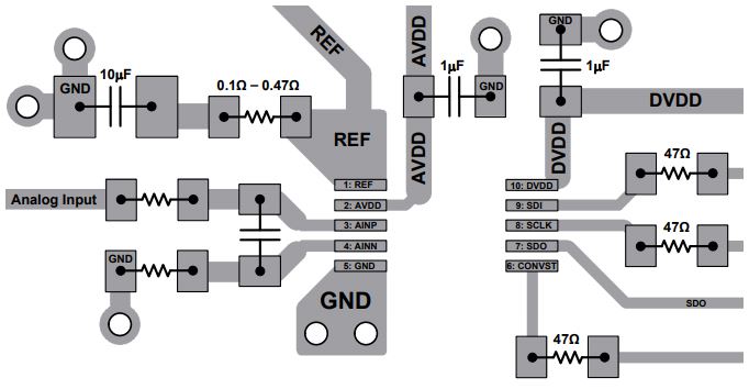
It is common sense to group analog and digital part separately. But in the case of ADC and DAC, it might be tricky some times. As these components have both the characteristics. We don’t want to create un-necessary interference of digital signal in the sensitive analog section. The best suggestion, in this case, is to follow the manufacturer reference design/app-note to achieve the best result. Although one can look at the previous designs also for reference. Some separation between analog and digital part is necessary. One can opt for place analog part and digital part on two sides of the IC. In some cases, their power supply may also be required to be Isolated.
3. Placement for routing
At this point, the intra-module intersection of signals has been minimized by grouping. Now its time to short out inter-module signal interaction. Air-wires in any CAD package are the signals. Arrange modules to minimise the signal crossing. in multilayer PCB with separate ground and power plane, these two signals can be ignored in placement. One may find that some updates in a grouping may be required. This process can be iterative with the aim of further optimization with every restructuring. Take special care for RF and Clock signals. Place components in such a manner that most of the RF signal path should be in a straight line (if possible also in one plane). Clock driver/synchronizer should be located close to clock oscillator. This will minimize skew as well as distortion.
4. Mind the aesthetics and accessibility
We don’t want our PCB to look messed up and randomly distributed. Do we? Good aesthetics might not make sense for functionality. but if one thinks in terms of debugging/testing and ease of assembly, it is more than important.
- Grid design: Use 50 or 100mil as the component grid to place these big components (QFP, BGA, SOP, SOIC, or through-hole connectors). Use 25mil as component gird for these SMT resistors/capacitors or other small passive components. If the board has space constraints use 25 mil grid and 5 mil grid for large and small component placement respectively. Using a grid system makes it easy while routing as we can rout most of them as straight lines which is always the best case.
- Component Direction: Arrange components in rows and columns, and oriented uniformly for ease of installation, inspection and rework. Point all polarized components such as tantrum capacitor and diodes in the same direction. The polarity of these components should be indicated on the silkscreen. If possible pin 1 of IC’s should also follow this guideline. This will result in a reduction of error probability while the assembly process.
- Give space to breathe: Keep at least 40mil space between components (keep at least 20 mils when space constraints are tight) and 100mil space from component to board edge. There should be enough space to route all the pins properly.
- One layer: Try to place all the components on the top side only. This will require only one pass-through during PCB assembly. If not possible, only low-profile, small size and low thermal dissipation component (like SMD passive parts) can be on the bottom side.
- Accessibility: Locate indication LEDs, test points, switches, jumpers and adjustable components for easy access.
5. Fine-tune the component placement for EMI/EMC requirements
The best PCB layout starts on the foundation of component placement. It is wise to not rush the process. Every extra iteration should add up niche a feature or remove a short-coming. There is always a chance for improvement in component placement. Once all components are placed there may be many areas for improvement at inter-module and intra-module level. Picking up a small detail and reducing the effort of routing by this creative process is the most challenging phase in PCB design life-cycle. But it’s totally worth it.
Taking the time to place the parts efficiently will result in a board, that works right out of the box. And that’s every engineer’s favorite moment.
Keep designing. Keep solving. And have fun in the process.
- 6 Steps of verification for error-free schematic
- 100 Point checklist for schematic design
- Selecting a PCB stack-up for EMC compliance
- Strategy for component placement
- Decoupling – Path to power integrity
- 15 PCB Layout guidelines to achieve EMC requirements
- 4 steps to review the PCB layout
- Checklist for error-free optimized PCB layout
- Engineered to doom – Red flags for PCB design
- Board bring up: Giving life to the design