Decoupling simply means the removal of undesired coupling. A simple example is a capacitor placed near power pin of an integrated circuit. It suppresses coupling between signals through power lines. Although it is not a process of just placing a capacitor. In more general sense decoupling points out to a method or practice by which one creates a reservoir to supply transient current requirements. It can be a simple capacitor, distributed capacitors or inductor-capacitor-resistor network. The aim is quite simple i.e. the effect of transient currents should not be visible on the power line. Smaller the effect of switching is there on a power line, smoother (less noisy) it performs. A constant DC on the power line of PCB will ensure that multiple IC can work together without interfering with each other.
Many people today are decoupling digital logic ICs by placing a single 0.1 or 0.01 uF capacitor next to the IC. This is the same method that has been used on digital logic ICs for the last forty plus years, so it still must be the correct approach — right! After all how much has IC technology changed in the last forty years? I think that it is interesting that this method has worked for as many years as it has. No one should be surprised that, possibly, we are now to the point that a new approach to decoupling is required.
Henry Ott
If considered properly it is the inductive and resistive part which is costing the power integrity in case of switching requirements. Resistance only limits the current supplied by a capacitor which may not be very significant many times. But the inductance presents the ultimate challenge. Some of the common inductance are mentioned in the table below.
| Source | Inductance | Remarks |
| Capacitor | 1 nH – 2 nH | Parasitic inductance |
| PCB Interconnects | 5 nH – 20 nH | Depends on Layout |
| Integrated Circuit | 300 pH – 15 nH | Bond wires and pins |
From table, we can safely assume that even for a good layout inductance may vary from 10 nH to 40 nH. And this is our limiting factor in the design. The designer has to think on all four fronts to achieve power integrity:
- Selection of components
- Component placement and
- PCB stack-up
- Routing
50 MHz and below
If considered all the harmonics (can limit up-to 5th) of fastest data signal or clock is below 50 MHz the usual method of placing capacitor near the power pin is sufficient enough. One or two (1uF or 0.01uF) capacitor should be enough to supply high current demand periods, preventing the voltage on the power supply rail from being pulled down by the momentary current load. The capacitor should be placed near the ground or power pin based on which layer is farther from the component. Generally, the ground layer is the nearest layer so the placement of decoupling capacitors near power leads are common. Placement of these should be based on the size of the loop area formed by capacitor and IC. Minimizing the area will result in better results.
50 MHz to 500 MHz
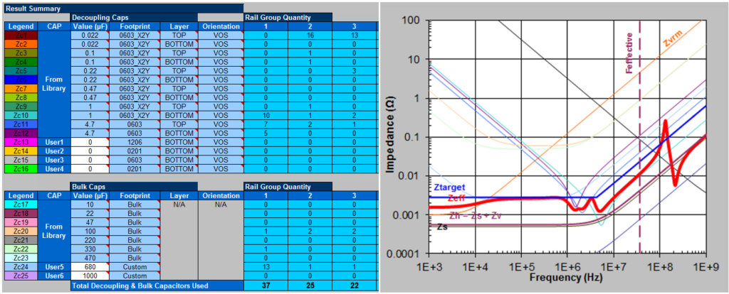
Above 50 MHz one or two capacitors may not be sufficient enough. There are multiple reasons for this: (a) Most of the capacitors resonant frequency fell in this band, (b) effect of inductance is magnified. A better strategy is to use multiple capacitors spread across to create some sort of distributed inter-plane capacitive network. This work due to the fact that when multiple LC network is placed in parallel, effective capacitance gets multiplied (C*n) by the number of repetition while effective inductance is divided (L/n). Both of these effects are in favour of power integrity. When using a large number of capacitors, the exact placement becomes less important than when using only one or two condensers. As for example, Intel recommends 41 decoupling capacitors for a Pentium 4 processor motherboard design. Although in this case manufacturer of chip will also help this process by providing multiple power and ground leads, distributed all around.
There are two school of thoughts in selection of capacitor values:
- The first school of thought recommends avoiding using different values for capacitors. Different value capacitors produce an anti-resonance, or cross-resonance,
which produces an impedance peak. A complex effect of resonance is something is to stay away from. For this purpose, a capacitor has to be chosen with resonance frequency above the desired frequency of operation (including harmonics). - The second school of thought recommends Different values of capacitors with their resonance frequency at different points so the impedance peak can be minimized. With this strategy, a lower resonant frequency capacitor can also be used but sufficient mathematics will be required to find out other capacitors which will nullify the effect. Multiple software packages can make it simple. One interesting example is the PDN tool from Intel to find out the optimum number of capacitors and their values for Intel chips.
500 MHz to 5 GHz
The effectiveness of the decoupling at high frequency is dependent on the number of capacitors used as opposed to the low frequency where it depends on the value of the capacitor used. Above 500 MHz the number of decoupling capacitor around the IC is not sufficient. At this instant, the complete board is needed to be converted to a distributed capacitive network. As a rule of thumb, a 1 uF (1 nF ideal capacitor) capacitor should be placed in every square inch of board space, along with the network around the IC discussed in the previous section. Due to the limit of the number of capacitors that can be used, it becomes more important to utilize interplane capacitance of PCB board itself. This results in an infinite number of infinitesimal capacitors spread all across evenly.
Zycon (which then became Hadco and is now Sanmina) developed a special PCB laminate in 1989-1990 with a 2-mil spacing between layers using standard dielectric FR-4 epoxy glass. This ZBC-2000 laminate provides 500 pF / sq. in. interplane capacitance. We can get the desired 1nF / sq by using two sets of power and ground planes in a PCB. This technology is also known as buried capacitance.
5 GHz and above
Above 5 GHz the buried capacitance becomes the necessity to provide sufficient decoupling. It is better to use a higher number of layers in stack-up with thinnest possible die-electric and multiple ground/power plane pair to provide inter-plane capacitance.
- 6 Steps of verification for error-free schematic
- 100 Point checklist for schematic design
- Selecting a PCB stack-up for EMC compliance
- Strategy for component placement
- Decoupling – Path to power integrity
- 15 PCB Layout guidelines to achieve EMC requirements
- 4 steps to review the PCB layout
- Checklist for error-free optimized PCB layout
- Engineered to doom – Red flags for PCB design
- Board bring up: Giving life to the design