Good PCB stack-up is very effective in reducing differential and common mode emission from the board. It is an important factor in quantifying the EMC performance of the product. Differential emission arises from the loop on PCB. These, in general, should be avoided during routing, but sometime it might not be possible to get rid of all such loops to attain the desired functionality. In such a case a well-planned PCB stack-up can conceal the emissions. On the other hand, wires connected to the board can give rise to common mode emission due to the potential difference between the ground returns. It can be minimized by careful component placement along with a solid ground layer.
Parameters for stack-up selection
EMC engineering expertise and experience of the design team is a crucial factor to achieve an optimum design in the lowest possible cost and time. Although new engineers with knowledge of electromagnetism, analog, and digital systems may also achieve commendable design by following standard practices and guidelines. To decide the factors involved in stack-up one need to consider the following.
- Number of signals to be routed and related cost
- Frequency of operation
- Emission requirements of the board
- If there is shielding or not for PCB
Factors to be decided
Based on parameters, the design engineer has to decide the number of layers, type of layers (Ground plane, Power Plane, signal layer, mixed layer) along with their sequence and spacing. It is suggested to finalize the first three factors early and have a rough idea about spacing. As spacing depends upon the properties of PCB material(e.g. dielectric constant, dissipation factor, permittivity, etc.) used hence it is better to contact the manufacturer at this stage. When provided with the rough stack-up idea along with the desired frequency of operation and current consumption on traces, PCB fabricator will be able to suggest the correct stack-up in optimum cost. Although the in-house team/designer can also use EM-solver to get the desired PCB stack-up with information about the capabilities of the manufacturer and the materials available.
Multi-layer Boards
Two-layer boards can be used up to 25 MHz and it may meet EMC compliance with a shielded enclosure. But as thumb rule boards with solid ground and power plane provide significant (up to 15 dB) reduction in radiated emission over two layer PCB. It is wise to use multi-layer boards above 10-15 MHz frequency range. With additional planes, signals can be routed in microstrip, strip-line or co-planer wave-guide structure. These impedance controlled configurations generate much less radiation than the random traces used in two layer board. In addition, ground noise is reduced considerably due to the decreased impedance of the return ground path.
Objectives to be achieved
When deciding on the PCB stack-up, an engineer has to strive for 5 golden objective which can improve the performance many-fold.
- Signal layers should be tightly coupled to their adjacent planes.
- Power and ground planes should be closely coupled.
- High speed signals should be routed in on buried layers.
- Multiple ground plane is advantageous in reducing the ground impedance further.
- From mechanical point of view if cross section of board is symmetric, it will prevent any wrapping.
In general 8 layers is the bare minimum requirement to meet all five objectives, but still, a good EMC compatible design can be achieved even in 4 or 6 layer boards with few compromises.
Engineering is a geek trade-off.
Eric Bogatin
In any selected number of layer, there may be many variants possible. We will look at some of them to develop an intuition which can be interpolated further for design specific needs. objectives which are fulfilled with the configuration are noted in braces.
4 Layer PCB stack-up

PCB_4LSU_1: It is obviously better than 2 layer PCB in terms of radiated emission. Although to provide mechanical strength layers are separated far and the desired coupling is not achieved. [obj. 5]
PCB_4LSU_2: This stack-up will further reduce the radiation up to 10 dB due to the increased coupling between the signal and their reference plane. For general designs, this PCB stack-up can be considered as optimal. [obj. 1, 5]
PCB_4LSU_3: This stack-up is pretty non-conventional. With component placement, there are multiple breaks in the upper/lower plane which makes the shielding below optimum. Some designers also worry about the power plane on external layers may be hazardous. [obj. 1, 3, 5]
PCB_4LSU_4: Upgrading above the third variant power and signal are placed on the same layer. Such an arrangement will be beneficial in case of connector cards. where mainly two connectors are placed on opposite sides of PCB, with few decoupling capacitors. [obj, 1, 3, 4, 5]
PCB_4LSU_5: A variation of PCB_4LSU_2 where power and signal are mixed on the top and bottom layer can be considered as the second optimum for general designs. It increases the ease of rework, although power may interfere with signals. [obj. 1, 5]
6 Layer PCB stack-up
The majority of six-layer boards consist of four layers of signal routing and two planes. Usually, a six-layer board is preferred over a four-layer board from an EMC perspective.
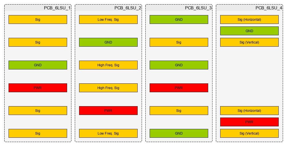
PCB_6LSU_1: This is an example of what not to use at all. Planes do not provide any shielding and signal layers are far from reference planes. [obj. 2, 5]
PCB_6LSU_2: This is the most common six-layer stack-up and can be very effective in controlling emissions. [obj. 1, 3, 5]
PCB_6LSU_3: This is one of the excellent performing stack-up variant but main issue arises due to smaller real estate for signal routing (only two layers) which can be challenging in many case. [obj. 1, 2, 3, 4, 5]
PCB_6LSU_4: This is a good stack-up although the separation between ground and power plane puts a strict requirement of solid decoupling. Also, the signals are crossing planes which have to be taken proper care of. [obj. 1, 4, 5]
8 Layer PCB stack-up
An eight-layer board can be used to add two more routing layers or to improve EMC performance by adding two more planes. The percentage increase in the cost of an eight-layer board over a six-layer board is less than the percentage increase in going from four to six layers, hence making it easier to justify the cost increase for improved EMC performance.

PCB_8LSU_1: This configuration satisfies all the objectives. Although when the high speed signal are changing layers a ground via should be provided adjacent to it. [obj. 1, 2, 3, 4, 5]
PCB_8LSU_2: This configuration adds two ground layers on top and bottom above PCB_6LSU_4. It is not commonly used but has the added advantage of routing orthogonal signals adjacent to the same plane. [obl. 1, 3, 4, 5]
PCB_8LSU_3: This configuration has the advantage of having a tightly coupled power-ground plane pair at the expense of not being able to shield the traces. [obj. 1, 2, 4, 5]
Takeaway
Choosing a PCB stack-up in the design process is analogs to the foundation for a house. Hence selecting it carefully can save a lot of costs afterward occurring towards mitigation of EMI/EMC issue.
- 6 Steps of verification for error-free schematic
- 100 Point checklist for schematic design
- Selecting a PCB stack-up for EMC compliance
- Strategy for component placement
- Decoupling – Path to power integrity
- 15 PCB Layout guidelines to achieve EMC requirements
- 4 steps to review the PCB layout
- Checklist for error-free optimized PCB layout
- Engineered to doom – Red flags for PCB design
- Board bring up: Giving life to the design